|
| |
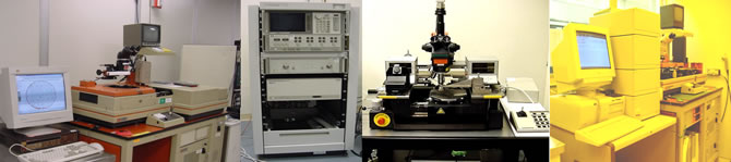
首頁 > 專業晶圓製造服務 > Foundry Services > Manufacturing Capabilities > Testing Capabilities |
|
| |
|
| |
|
| |
- 100% on-wafer Automated DC and RF Testing
- DC (die sorting)
- RF (up to 20 GHz): OIP3, harmonics, Oscillator, S-parameters, etc.
- Engineering Characterization Support (Up to 40 GHz)
- Device Modeling (linear and non-linear models)
- DC parametric test
- RF small signal/large signal characterizations (load pull, OIP3, noise parameters etc.)
- Automatic Wafer Mapping With Ink or Inkless Electronic Wafer Mapping
|
|
|
|